Product Summary
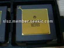
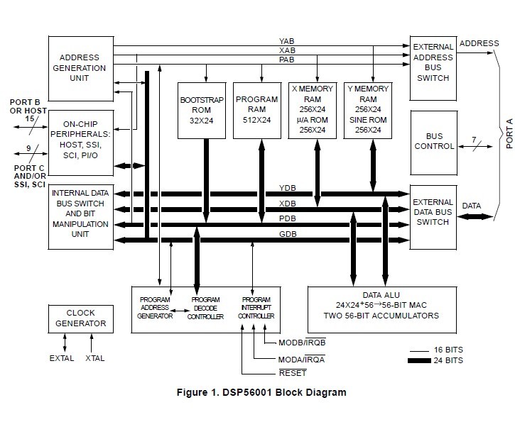
The DSP56001RC20 is a member of Motorola’s family of HCMOS, low-power, general purpose Digital Signal Processors. It is an off-the-shelf part since the program memory is user programmable. The core of the processor includes three execution units operating in parallel — the data ALU, the address generation unit, and the program controller. In addition, the device has MCU-style on-chip peripherals, program and data memory, as well as a memory expansion port. With high throughput, it is suitable for communication, high-speed control, numeric processing, computer and audio applications. It is available in PGA package.
Parametrics
Maximum Ratings: (1)Supply Voltage, Vcc: -0.3 to +7.0 V; (2)All Input Voltages, Vin: VSS- 0.5 to Vcc + 0.5 V; (3)Current Drain per Pin excluding Vcc and VSS, I: 10 mA; (4)Operating Temperature Range, TJ: -40 to +105℃; (5)Storage Temperature, Tstg: -55 to +150℃.
Features
Key Features: (1)Speed: At 16.5 million instructions per second (MIPS) with a 33 MHz clock, the DSP56001 can execute a 1024 point complex Fast Fourier Transform in1.98 milliseconds (66,240 clock cycles).; (2)Precision: The data paths are 24 bits wide thereby providing 144 dB of dynamic range; intermediate results held in the 56-bit accumulators can range over 336 dB; (3)Parallelism: The data ALU, address arithmetic units, and program controller operate in parallel so that an instruction prefetch, a 24x24-bit multiplication, a 56-bit addition, two data moves, and two address pointer updates using one of three types of arithmetic (linear, modulo, or reverse carry) can be executed in a single instruction cycle. This parallelism allows a four coefficient Infinite Impulse Response (IIR) filter section to be executed in only four cycles, the theoretical minimum for a single multiplier architecture; (4)Integration: In addition to the three independent execution units, the DSP56001 has six on-chip memories, three on-chip MCU style peripherals (Serial Communication Interface, Synchronous Serial Interface, and Host Interface), a clock generator and seven buses (three address and four data), making the overall system functionally complete and powerful, but also very low cost, low power, and compact; (5)Invisible Pipeline: The three-stage instruction pipeline is essentially invisible to the programmer thus allowing straightforward program development in either assembly language or a high-level language such as ANSI C.
Diagrams
 |
 DSP56001 |
 Other |
 |
 Data Sheet |
 Negotiable |
|
||||
 |
 DSP56001A |
 Other |
 |
 Data Sheet |
 Negotiable |
|
||||
 |
 DSP56002 |
 Other |
 |
 Data Sheet |
 Negotiable |
|
||||
 |
 DSP56004 |
 Other |
 |
 Data Sheet |
 Negotiable |
|
||||
 |
 DSP56005 |
 Other |
 |
 Data Sheet |
 Negotiable |
|
||||
 |
 DSP56007 |
 Other |
 |
 Data Sheet |
 Negotiable |
|
||||
 (China (Mainland))


